
Common circuit structure in desktop power adapters
The three most common structural layouts of desktop power adapters are buck, boost, and buck-boost, none of which are isolated from each other. the boost converter (or step-up converter) is a common switching DC boost circuit, which can make the output voltage higher than the input voltage. The following is mainly from the basic principle, boost circuit parameter design, how to Boost circuit protection circuit three aspects to describe.
Basic principle analysis of Boost circuit
The Boost circuit is a switching DC boost circuit that makes the output voltage higher than the input voltage. It is a common circuit design method in electronic circuit design.
First, you need to know the basics:
Capacitors block voltage changes: through high frequencies, blocking low frequencies, through AC, blocking DC;
Inductance blocks current changes: through low frequency, block high frequency, through DC, block AC;
Suppose (1) the switching tube (transistor or MOS tube) has been disconnected for a long time, all the components are in an ideal state, and the capacitor voltage is equal to the input voltage. The following is divided into charging and discharging two parts to explain this circuit.
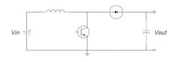
1. Charging process
During the charging process, the switch is closed (triode conduction), the equivalent circuit is shown in Figure (2), and the switch (triode) is replaced by a wire. At this time, the input voltage flows through the inductor. The diode prevents the capacitor from discharging to the ground. Since the input is direct current, the current on the inductor increases linearly at a certain ratio, which is related to the size of the inductor. As the inductor current increases, some energy is stored in the inductor.
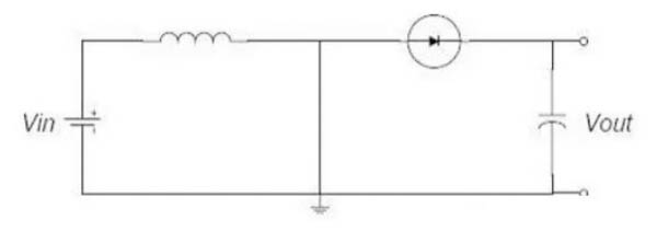
2. Discharge process
As shown in Figure (3), this is the equivalent circuit when the switch is off (triode cutoff). When the switch is turned off (transistor cut-off), due to the current holding characteristics of the inductor, the current flowing through the inductor does not immediately change to 0, but slowly changes from the value at the end of charging. The original circuit has been disconnected, so the inductor can only discharge through the new circuit, that is, the inductor begins to charge the capacitor, the voltage at both ends of the capacitor rises, and the voltage is already higher than the input voltage. The boost is complete.
Speaking of the voltage boost process is an inductive energy transfer process. When charging, the inductor absorbs energy, and when discharging, the inductor emits energy. If the capacitance is large enough, a continuous current can be maintained at the output end during discharge. If this on-off process is repeated, a voltage higher than the input voltage can be obtained at both ends of the capacitor.
Design of Boost circuit parameters
For Boost circuits, the inductance current continuous mode is very different from the inductance current discontinuous mode. The discontinuous mode output voltage is related to the input voltage, inductance, load resistance, duty cycle, and switching frequency. The output voltage of continuous mode depends only on the input voltage and duty cycle.
1. Selection of output filter capacitance
In a desktop power adapter, the role of the output capacitor is to store energy and maintain a constant voltage.
The capacitor selection of the Boost circuit is mainly to control the ripple of the output within the range specified by the indicator. For Boost circuits, the impedance of the capacitor and the output current determine the size of the output voltage ripple. The impedance of a capacitor consists of three parts, namely the equivalent series inductance (ESL), the equivalent series resistance (ESR), and the capacitance value (C). In inductive current continuous mode, the size of the capacitor depends on the output current, switching frequency, and desired output ripple. When the MOSFET is turned on, the output filter capacitor provides the entire load current.
2. Inductance
In a desktop power adapter, the role of the inductor is to store energy. The function of the inductor is to maintain a constant current, or to limit the change of current in the inductor. In a Boost circuit, choosing the appropriate inductance is usually used to limit the ripple current flowing through it. The ripple current of the inductor is proportional to the input voltage and MOSFET on-time, and inversely proportional to the inductance. The amount of inductance determines the operating point of continuous mode and non-continuous mode. In addition to the inductance of the inductor, the selection of inductors should also pay attention to its maximum direct current or peak current, and the maximum operating frequency. The inductance current exceeds its rated current or the operating frequency exceeds its maximum operating frequency, which will lead to inductance saturation and overheating.
3.MOSFET
In low-power DC/DC variations, Power MOSFETs are the most commonly used power switches. The cost of MOSFET is relatively low, and the operating frequency is relatively high. The selection of MOSFET in the design mainly considers its on-loss and switching loss.
The MOSFETs are required to have a sufficiently low on-resistance RDS (ON) and a relatively low gate charge Qg.
Jptpower is a leading manufacturer of desktop power adapter in China. We provide machining power adapter service, Today, we are providing high-quality desktop power adapter to more than clients all over the world.
Put protective clothing on the Boost circuit
In the previous part, we understand the Boost circuit and the design of the Boost circuit parameters from the point of view of charge and discharge.
Boost circuit as a non-isolated boost circuit, its structure is simple, easy to design, low cost, is widely used in a variety of do not need isolation boost occasions, especially in the active PFC circuit is the most widely used.
The BOOST circuit seems to be more cumbersome to protect than BUCK or other isolation circuits. For the general protection circuit, when the input under voltage, overvoltage, output over current, short circuit, overvoltage, over temperature, we will require the circuit will automatically turn off the output, or achieve burp-type protection, in order to facilitate the following load or circuit to be protected in time to avoid damage; However, for the BOOST circuit, due to the boost inductance, the output rectifier diode is in series in the input and output loop, even if the MOSFET is completely turned off, the output will have a voltage lower than the input voltage inductor DC voltage drop and the diode positive voltage drop, which means that the output cannot be completely turned off, and the protection effect we want is not achieved. There are several solutions that can be used to protect BOOST circuits.
1. MOS can be added to the input end for shutdown protection. This is a good method, but the control of MOSFET is more complex, and requires high voltage and high current MOSFET, which will increase the cost of the system and reduce reliability. The result is that the input voltage is relatively low, and the input voltage is more convenient to achieve soft start and reduce the impact on MOS. However, since the output current is smaller, the MOS power consumption is smaller when added to the output.
2. For similar products, Japan requires that the output side must have an insurance device, usually a recoverable fuse. Recoverable fuse is PTC, not suitable for high-power occasions, and will produce a lot of loss, the insurance device added to the output than the input loss is relatively small, and this way the cost is lower and economical.
3. It can be used in the way of serial relay on the bus, while turning off the MOS, synchronously cut off the relay, so that the winner loop can be disconnected to cut off the current loop and further protect the diode. Relays are a common protection method, but they also have disadvantages such as short life and easy ignition when switching.
4. If you do not consider the cost and complexity, the perfect protection circuit can be done! But in fact, the output short circuit is an individual case, and the excessive cost of this “accident” is very not worth it.
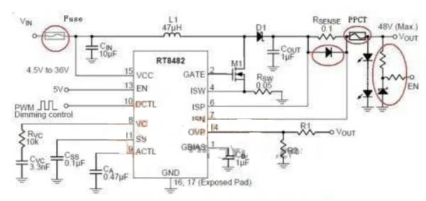
4.1 Fuse must be available at the Vin end to prevent MOS breakdown from causing security risks.
4.2 When the output is short-circuited, the fragile parts that are affected by high current need to be strengthened (Rsense in the figure).
4.3 BOOST output current is often much less than the input current, much less than the high current in the short circuit, so the use of PPTC (self-restoring fuse) is feasible. PPTC action current can be 2 to 3 times the output current, normal, PPTC loss is very small.
4.4 Boost enables the pin EN voltage to be taken from the output, but after a short circuit, EN=0V (voltage drop on PPTC), the IC immediately stops working, the output voltage is reduced to about equal to the input voltage, which can reduce the power consumption after short circuit protection, but also reduce the voltage at both ends of PPTC, to reduce the power consumption of PPTC.
5, when the output short circuit is eliminated, due to the presence of PPTC, EN re-power, IC start, BOOST work again.
At present, few people pay attention to this piece, even the current PFC circuit launched by major manufacturers, as long as the post-stage a short circuit, the consequences can be imagined. The safest way to protect is to cut off the input, the current switching devices have transistors, MOSFET, IGBT, relays, contactors, etc., different switching devices have different advantages and disadvantages.
Recommended products
Conclusion
In summary, the common circuit structures in desktop power adapters include buck (buck), boost (boost) and buck-boost (buck-boost). In these structures, the Boost circuit is a common switching DC boost circuit, which is able to make the output voltage higher than the input voltage.
The basic principle of the Boost circuit is to transfer energy through the inductor, the inductor absorbs energy during the charging process, and the inductor releases energy during the discharge process, thereby achieving a voltage increase. When designing the Boost circuit, it is necessary to consider the choice of output filter capacitance, the suitability of inductance, and the on-loss and switching loss of MOSFET.In addition, in order to protect the Boost circuit, you can install MOS switches, recoverable fuses, relays and other measures. In short, as a non-isolated booster circuit, the Boost circuit has certain challenges in design and protection, but through appropriate parameter design and protection measures, it can ensure its stable and reliable work.
It should be noted that different protection methods have their own advantages and disadvantages, and should be selected and weighed according to actual needs. It is worth mentioning that China’s Power adapter supplier JPT Power has rich experience and technical strength in this field, providing users with high-quality desktop power adapter products and solutions.